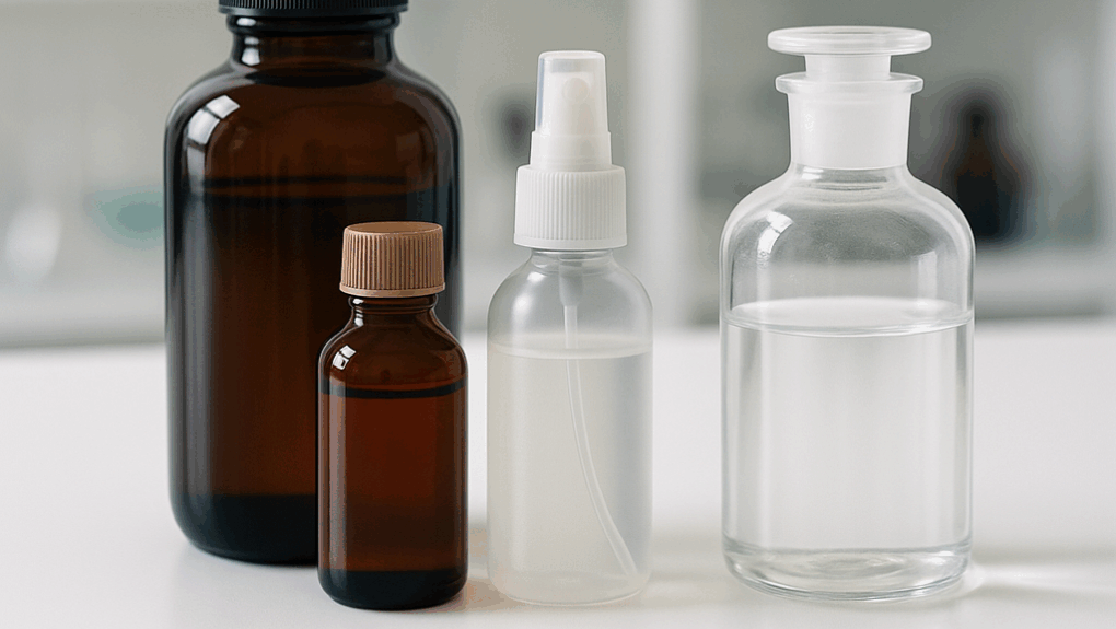
Trimethyl Borate (TMB)
High-purity boron compound for advanced BPSG deposition.
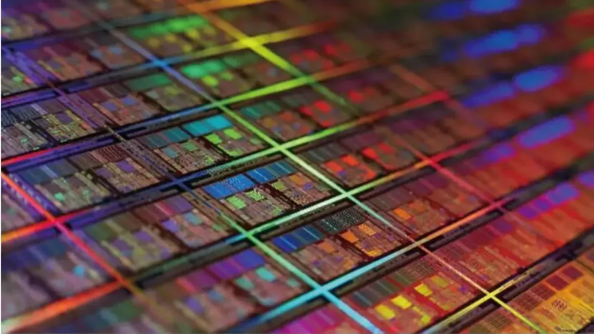
Enables clean doping and dielectric layering in wafer processing and MEMS production.
Versatile Boron Precursor for Glass Formation and Doping Applications
Trimethyl Borate (TMB) is a high-purity boron compound used as a key dopant source in the formation of boro-phospho-silicate glass (BPSG) layers via chemical vapor deposition (CVD). These boron-enriched dielectric layers improve flow properties and stress control in semiconductor devices and are essential for modern ICs, MEMS, and discrete components.
Due to its high volatility, clean decomposition, and low impurity levels, TMB is widely used in wafer fabrication processes requiring precise and uniform boron incorporation.
NAGASE supplies Trimethyl Borate in electronic-grade quality for global semiconductor, MEMS, and microelectronics applications – with full technical support and international logistics capabilities.
Chemical Formula: B(OCH3)3
Molecular Weight: 103.92
Physical & Chemical Properties
A colorless liquid without significant odor. Stable in normal condition.
Melting Point: -29℃
Density: 0.915g/ml
Boiling Point: 67~68℃. Flammable and reacts violently with oxidants. It can be hydrolyzed into Methanol and Boric Acid. Miscible with organic solvents.
Applications
Trimethyl Borate is mainly used for BPSG deposition in semiconductor wafer processing.
- Deposition of BPSG dielectric layers
- Wafer fabrication processes for IC and memory devices
- Semiconductor manufacturing requiring boron doping
- Production of MEMS and microcomponents
- Integration into discrete devices
Features
Trimethyl Borate provides high boron purity, excellent volatility, and compatibility with advanced CVD processes for BPSG applications.
- Electronic-grade quality – Low impurity levels for critical semiconductor use
- High boron content for effective doping and dielectric modification
- Excellent volatility – Enables uniform gas-phase deposition
- Thermally stable – Clean decomposition under CVD conditions
- Global availability – Supplied by NAGASE with full technical support
Product Specification
| Product | 8.5N | ||
|---|---|---|---|
| Purity (based on metals analyzed), min | 99.9999995 % | ||
| (Al)max | 0.1 ppb | (Pt)max | 0.05 ppb |
| (Sb)max | 0.1 ppb | (K)max | 0.2 ppb |
| (As)max | 0.2 ppb | (Re)max | 0.05 ppb |
| (Ba)max | 0.05 ppb | (Rh)max | 0.05 ppb |
| (Be)max | 0.05 ppb | (Rb)max | 0.05 ppb |
| (Bi)max | 0.05 ppb | (Ag) max | 0.1 ppb |
| (Cd)max | 0.05 ppb | (Na)max | 0.3 ppb |
| (Ca)max | 0.5 ppb | (Sr)max | 0.05 ppb |
| (Ce)max | 0.05 ppb | (Ta)max | 0.05 ppb |
| (Cr)max | 0.05 ppb | (Tl)max | 0.05 ppb |
| (Co)max | 0.05 ppb | (Th)max | 0.05 ppb |
| (Cu)max | 0.1 ppb | (Sn)max | 0.05 ppb |
| (Ga)max | 0.1 ppb | (Ti)max | 0.05 ppb |
| (Ge)max | 0.05 ppb | (W )max | 0.05 ppb |
| (Au)max | 0.1 ppb | (U )max | 0.05 ppb |
| (Hf)max | 0.05 ppb | (V) max | 0.05 ppb |
| (In)max | 0.05 ppb | (Zn)max | 0.2 ppb |
| (Ir)max | 0.05 ppb | (Zr)max | 0.05 ppb |
| (Fe)max | 0.3 ppb | (B )max | 0.5 ppb |
| (Pb)max | 0.1 ppb | Cl- max | 50 ppb |
| (Li)max | 0.05 ppb | Water max | 20 ppm |
| (Mg)max | 0.2 ppb | Particle ≥0.2 µm max | 10 p/ml |
| (Mn)max | 0.1 ppb | Particle ≥0.3 µm max | 7 p/ml |
| (Hg)max | 0.1 ppb | Particle ≥0.5 µm max | 5 p/ml |
| (Mo)max | 0.1 ppb | Particle ≥1.0 µm max | 1 p/ml |
| (Ni)max | 0.1 ppb | Assay min | 99.99% |
| (Nb)max | 0.05 ppb | Chroma max | 5APHA |
| (Pd)max | 0.05 ppb | Shelf life | 24 months |
Packaging Size
Container: Stainless Steel Cylinder
Packaging: Stainless Steel Cabinet
Fill volume: 2 gallons,5 gallons (19 L),10 gallons
Frequently Asked Questions about Trimethyl Borate (TMB)
What is Trimethyl Borate (TMB) used for in semiconductor manufacturing?
TMB is primarily used as a boron source for forming BPSG dielectric layers via chemical vapor deposition in wafer fabrication.
Why is BPSG important in integrated circuit production?
BPSG layers improve planarization, reduce topography, and enhance the flow properties of interlayer dielectrics in semiconductor devices.
How does TMB behave in CVD processes?
Due to its volatility and clean thermal decomposition, TMB enables precise control of boron incorporation during CVD, resulting in uniform thin films.
Can TMB be used in MEMS and discrete device manufacturing?
Yes, TMB is widely used in the production of MEMS and discrete components where boron-doped dielectrics are required.
What are the advantages of using high-purity TMB?
High-purity TMB ensures minimal contamination and defect formation during deposition, making it suitable for high-end semiconductor applications.
Related Products
Trimethyl Phosphite (TMP)
High-purity phosphorus precursor for PSG and BPSG layer formation. Enables controlled doping and dielectric deposition in advanced semiconductor manufacturing.
Trimethyl Phosphate (TMPO)
High-purity phosphorus ester for PSG and BPSG deposition. Enables precise dielectric layering in wafer fabrication and microelectronics production.
Triethyl Phosphate (TEPO)
High-purity phosphorus ester for PSG & BPSG deposition. Enables precise dielectric layering in advanced semiconductor manufacturing.

Triethyl Borate (TEB)
High-purity boron ester for advanced chemical applications. Nagase supplies triethyl borate (TEB) used in organic synthesis, cross-coupling reactions, and specialty solvent systems where boron precision is essential.
Trans-1,2-Dichloroethylene (DCE)
High-purity solvent for efficient surface treatment. Nagase delivers trans-1,2-dichloroethylene (DCE) used in polymer production, metal degreasing, and electronics cleaning where performance and purity are critical.
Tetraethyl Orthosilicate (TEOS)
Reliable performance for next-generation semiconductor fabrication. Nagase's high-purity TEOS ensures optimal film quality, consistency, and reliability across a wide range of deposition environments.
Red Phosphorus
High-purity phosphorus for safety and innovation. Nagase delivers red phosphorus in electronic and industrial grades for flame retardants, semiconductor doping, and specialized materials.
Phosphorus Pentoxide
Powerful dehydration meets phosphorus chemistry. Nagase supplies high-purity P₂O₅ for use in electronics, fine chemical synthesis, and phosphorus-based compound production.

Phosphorus Oxychloride (POCl3)
Reliable reactivity for high-tech manufacturing. Nagase offers POCl₃ in electronic and industrial grades for diffusion doping, phosphorylation reactions, and advanced chemical processes.

Boron Tribromide
Reliable performance for sensitive chemical processes. Nagase supplies high-purity boron tribromide (BBr₃) for advanced synthesis, demethylation, and semiconductor applications.
